
South Korean Researchers Target 2030 for Scalable 2D Semiconductor Production

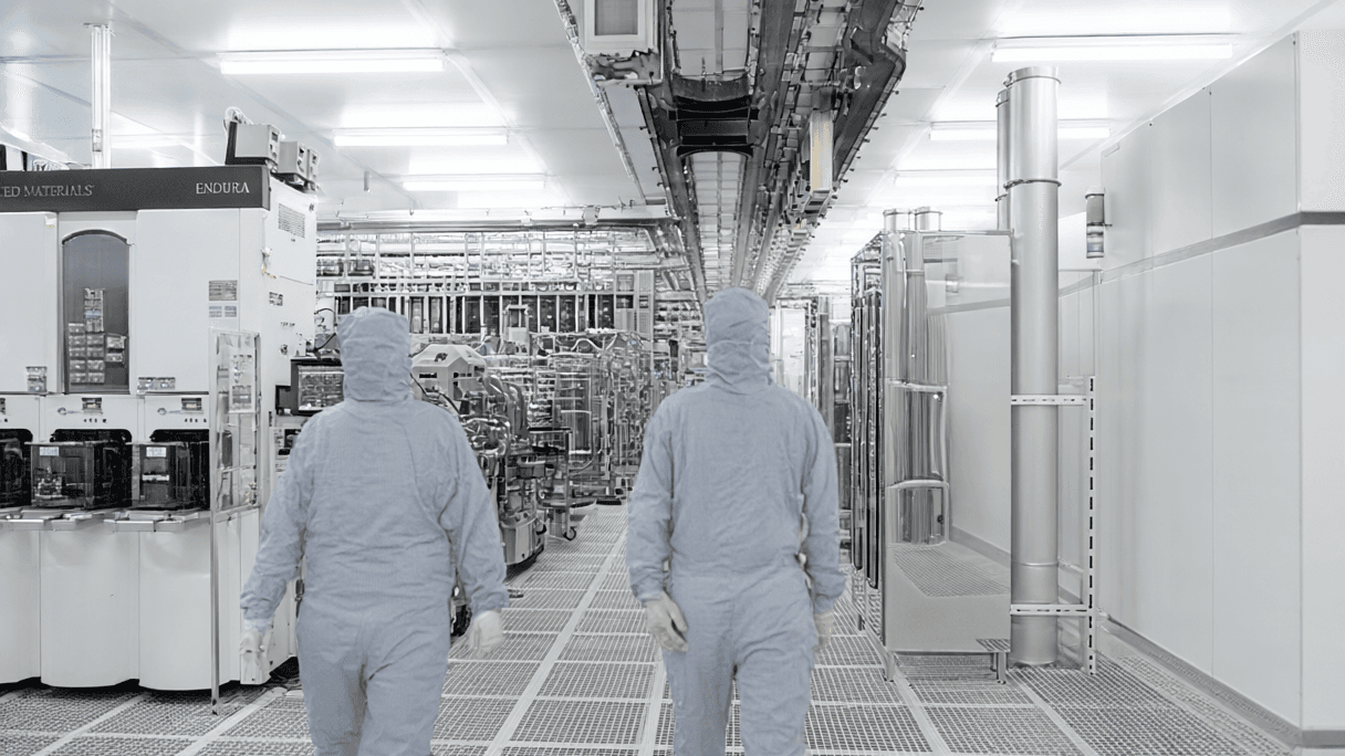
AI-generated image · US National Wire
A new etching-flux process aims to solve the random crystal growth that has hindered the commercialization of atomically thin semiconductors.
Researchers from KAIST and the South Korean startup TDS Innovation have developed a method to control the growth of 2D semiconductor crystals, a critical step toward manufacturing next-generation chips at scale, as first reported by The Register.
As detailed in a study published in *Nature* on October 7, the team utilized an "etching-flux-mediated single-centred nucleation" (EF-SCN) process. This technique uses oxygen released from an oxide barrier to create a lateral etching flux, which prevents crystals from forming randomly across a growth region and instead restricts growth to the geometric center. This addresses a primary manufacturing hurdle: when multiple crystals form and merge, they create boundaries that degrade electrical performance.
In tests conducted on a two-centimeter substrate, the process achieved a 99.3 percent yield, creating single crystals at 397 out of 400 patterned sites. The researchers used this method to build field-effect transistors (FETs) using molybdenum disulfide (MoS₂), reporting higher charge-carrier mobility than previous selectively grown versions of these transistors.
From a deployment perspective, the goal is to integrate 2D semiconductor devices onto silicon chips to bring logic and memory closer together. According to TDS Innovation, this would reduce the energy and time required to move data. The technology is also being explored for complementary field-effect transistors (CFETs), a 3D stacking method previously demonstrated by Intel and IBM.
While the study does not specify a production date, Jony Jung of TDS Innovation told The Register the company is aiming for commercial use around 2030, noting that demand from robotics and AI could potentially accelerate this timeline.